DSGW-390 Mobile Charging Robot Main Controller

The DSGW-390 is designed based on the Rockchip RK3588J, equipped with an 8-core CPU, 6TOPS of independent NPU computing power, and powerful AI functionality. It includes a variety of peripheral interfaces such as USB, LVDS, HDMI, and CAN, fully meeting the connection requirements of a robot's multi-sensor perception and control modules.
Table of Contents

1.Product Introduction

1.1Product Overview

Product overview based on Rockchip RK3588J Designed for Mobile charging robot A high-performance Main control box products. DSGW-390 has an 8-core CPU, 6TOPS independent NPU computing power, strong AI capabilities, and includes rich peripheral interfaces such as USB, LVDS, HMDI, CAN, etc., fully meeting Access requirements for robot multi-sensor perception and control blocks The product meets industrial design standards and adopts metal casing and Anti-vibration interface design, applicable to Outdoor, industrial, severe vibration of the whole machine It supports flexible selection of operating systems, with Ubuntu system as standard, and can also independently run Android / Linux+RTOS fusion operating system. It is mainly used in robot scenarios that require high performance and high computing power, such as mobile charging robots and service robots.

1.2 Hardware Specifications
name describe
Product Model DSGW-390
CPU RK3588J
RAM 8GB
EMMC 64GB
system Ubuntu 20.04
Network port 1 10/100/1000Mbps Ethernet interface
USB interface 3* USB 2.0 +1* USB 3.0 Type A
1* USB Type C
WI-FI Wifi6, 802.11a/b/g/n/ac/ax 1200Mbps WLAN + BT v5.2
wireless Support private Lora
Audio Support, dual channel output
video Support, 1 LVDS interface, 1 HDMI interface
RTC support,
Debug interface Support, Phoenix terminal
Cooling Solution Support radiator
IO interface DI,DO,AI, PWM, isolation
CAN 3-way, isolated
RS485 1-way, isolated
power supply DC power supply voltage range 9~16VDC
Operating temperature -40 to 85 degrees
Storage temperature -40 to 105 degrees
PCBA Dimensions 208.3*147mm
1.3 Product Application Diagram
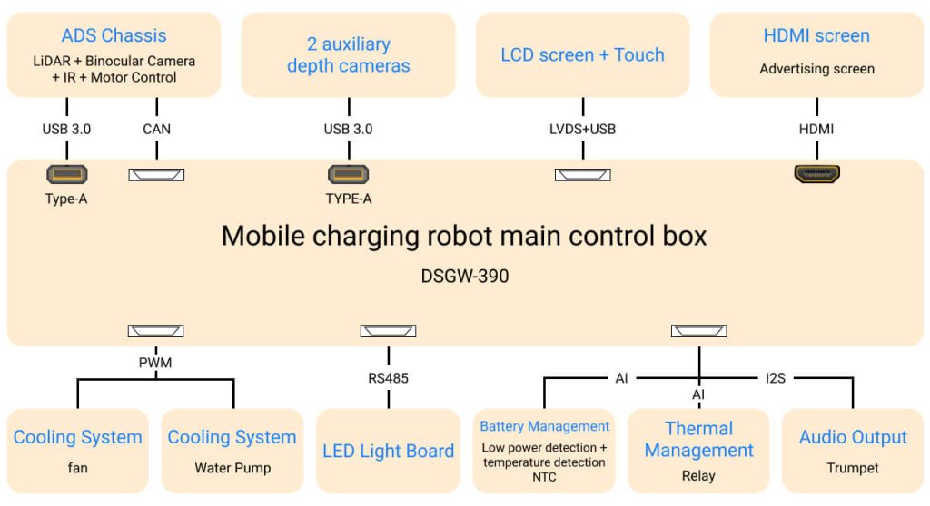
1.3.1 Hardware Application Block Diagram
dsgw 390 hardware application block diagram
1.3.2 System Software Block Diagram

Dusun integrates the robot main control box industry-related applications on the basis of the standard system, customizes a highly reliable operating system and industry SDK, and completes the transplantation and testing of a variety of hardware peripheral drivers that meet industry applications with many years of experience in the development and design of robot embedded motherboards. The following is the system software framework

dsgw 390 system software block diagram

In addition, Dongsheng can provide independent system support for various versions of Linux, such as Debian, Ubuntu, Openwrt, etc.
Dongsheng provides the robot master control box industry SDK source code that matches the motherboard, supporting customers to conduct micro-development to achieve rapid productization. Dongsheng Robot Industry SDK has the following features:
1. Streamlined operating system: On the premise of meeting industry applications, the number of components is streamlined, the system resource utilization rate is high, thereby reducing hardware costs, and to a certain extent, the functional structure is optimized, the system architecture is reasonably laid out, and the system is more efficient and easy to maintain;
2. BSP with industry attributes: According to the types of peripheral devices used in the industry, it supports multiple sensor interfaces to facilitate the connection of sensors such as cameras, lidars, IMUs, and supports multi-screen display drivers, as well as multi-channel DIO.AIO for battery management, whole-machine heat dissipation management, whole-machine thermal management, etc. It performs driver transplantation and debugging and adapts industry algorithms to meet customers’ needs for the overall hardware + algorithm solution. In addition, Dongsheng BSP driver will continue to iterate the access of peripheral devices of different brands and models.
3. Pre-installed tools and middleware: Pre-install NPU’s big data model tools (such as ONXX, etc.) and the middleware ROS/ROS2 of the robotics industry in advance, so that users can quickly transplant applications and tree models of other hardware platforms and achieve low-cost hardware platform switching.

1.3.3 Supported algorithms and peripheral hardware
1.3.3.1 Basic equipment
Peripherals model illustrate
fan 013102018
Support PWM speed control
Support speed FG signal reading back
Water Pump 043100010 Support PWM speed control
Support speed FG signal reading back
trumpet - 8W speaker
Relay AP24512ABDNil60
NTC PT100
USB Camera - Universal UVC
External expansion USB flash drive TinkPad/Patriot/Kingston mainstream models Universal 3.0/2.0 USB flash drive
Advertising screen - HDMI standard display
Car display screen AV123Z7M-N12 (BOE) Size 12.3 inches, resolution 1920*720, refresh rate 60Hz,
1.3.3.2 Core Components
Core Algorithm Matching peripheral hardware model illustrate
SLAM Algorithm LiDAR+Binocular Camera+Motor SLAMTEC Athena Robot chassis
Face recognition algorithm Structured light module RMSL321 RK NN Deep Algorithm
Intelligent voice algorithm 6-microphone circular array Can be customized according to structure Sound pickup and noise reduction, keyword wake-up, voice wake-up
Monocular ranging algorithm Structured light module RMSL321 Distance and angle information of visual obstructions

Note: The above algorithms are not pre-installed in the factory firmware version. If necessary, please contact the corresponding technical window

1.3.3.3 Supported algorithm models

ROS (Robot Operating System) is pre-installed in the product SDK. As the de facto standard operating system in the field of robotics, ROS provides a wealth of tools and libraries for building complex robotic systems. Pre-installing ROS on RK3588J can greatly simplify the robot development process.

1.4 Hardware Description
  • RK3588J industrial-grade high-performance CPU, integrated with quad-core A76 and quad-core A55 processors, with a maximum main frequency of 2.4GHz;
  • G610 MP4 GPU and 6TOPS NPU, providing powerful computing power and graphics and video processing capabilities;
  • Support 4G LTE CAT4 (China);
  • Supports Wi-Fi 5 and Bluetooth 4.2;
  • Provide powerful computing performance and high-performance processing resources for AI edge computing;
  • Support industrial bus protocols such as CAN, RS485;
  • Supports a variety of isolated DIO and AIO interfaces;
  • Support private wireless protocols, such as LoRa private protocol;
1.5 Hardware Specifications
Name Describe External interface form Remark
Product Model DSGW-390
CPU RK3588J On the core board The core board is mounted on the main board via four board-to-board connectors
RAM 8GB
EMMC 64GB
HDMI interface 2 HDMI ports Externally use Type A interface
Network port 1 10/100/1000Mbps Ethernet interface Using RJ45
USB3.0 interface 1 USB3.0 HOST interface 1-way USB 3.0 HOST uses USB 3.0 Type A female connector
USB2.0 interface 3-way USB2.0 HOST interface 3-way USB2.0 HOST uses USB2.0 Type A female connector
LTE LTE 4G CAT4 with main antenna, diversity antenna and GPS antenna Connect an external antenna via a BNC connector
LORA The frequency band of Lora on the device side is 470MHz Connect an external antenna via a BNC connector
Wifi Wifi5, IEEE 802.11a/b/g/n/ac 433.3Mbps WLAN + BT v4.2, SDIO interface, 1 BNC antenna socket Connect an external antenna via a BNC connector
Audio 2 speaker driver interfaces, can drive 2 8 ohm/3W speakers External use of 2*2Pin connector
DP screen interface Use the DP interface and multiplex it with the firmware burning interface External use Type C female connector
LVDS screen interface 2 groups of LVDS interfaces, 4 pairs of signal lines in each group, 51Pin connector One 51-pin socket for external use
LVDS screen touch interface USB2.0 HOST interface, using connector
LVDS screen backlight driver interface Use PWM to drive the brightness of the screen One 14-pin socket for external use
LVDS screen temperature detection interface Use NTC temperature sensor to measure the temperature of the screen
RS485 1 RS485 interface External use of 2*4Pin connector
CAN interface 3-way CAN interface
Digital input 3-way passive digital input interface External use 6Pin connector
Digital output 5-channel digital output interface External use 5Pin connector
PWM Output 2-way PWM output interface External use 2Pin connector
External temperature detection interface 2-way NTC temperature measurement interface External use 4Pin connector
RTC 1 real-time clock chip No external
Debug port 1 UART interface, CMOS level, level 3.3V, 2.54mm pitch, 3Pin socket External use 3pin socket
button 1 hard reset button
1 RECOVERY button
1 MASKROM button
fan Core board cooling fan interface, 1.25mm spacing, 4Pin socket Use within the board Reserved fan socket
Firmware burning interface Software program used to burn PCBA, reused with DP screen interface External use Type C female connector
power supply Battery powered, voltage range 9V to 12V, 60W Powered by 2Pin connector
Operating temperature -40 to 85 degrees
Storage temperature -40 to 85 degrees
PCBA Dimensions 208.3*147mm

2. Installation Instructions

2.1 Packaging instructions

⚠️:This section describes the product packaging form (boxed/antistatic bag, etc.?), packaging size, unit weight, packing instructions, etc.

  1. Product shipping box type: None.
  2. Product shipping packaging bag type: PE flat bag.
  3. Weight of complete stand-alone machine (excluding accessories): 1500g±10g.
  4. Description of packing: 4 units per box, the packing box is in the form of top and bottom box + pearl cotton.
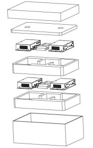
dsgw 390 packaging instructions
2.2 Accessories List

⚠️:This section describes the factory accessories list of the product

  1. Product has no accessories.
2.3 Installation

⚠️:This section describes the installation method and installation precautions of the product. If the product is a complete machine, use diagrams to describe the appropriate installation method and installation steps. If the product is a PCBA, describe the fixed space and air avoidance rules, radiator installation, etc.

  1. The product is installed by fixing it on the product with corresponding screw posts through M6 screws. Or the product can be fastened to the plate through the combination of M6 screws + M6 nuts, but it should be noted that holes that can pass the screws must be reserved on the plate.
dsgw 390 installation
2.4 Product Dimensions

⚠️: Use 2D wireframes to quickly describe the product dimensions. Also provide a link to download the 3D product image.
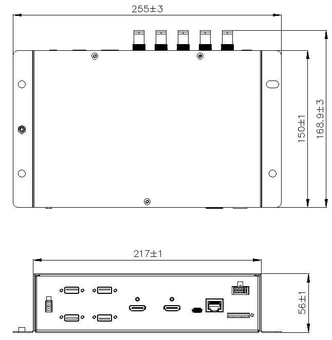
dsgw 390 product dimensions

3. Hardware Instructions

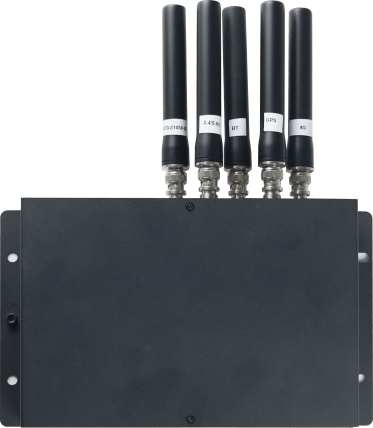
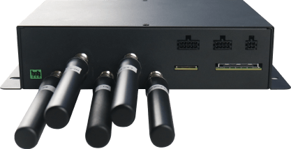
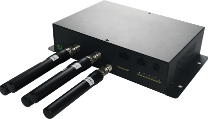
3.1 Product Appearance
DSGW 390 2
DSGW 390 1
DSGW 390 3
DSGW 390 4
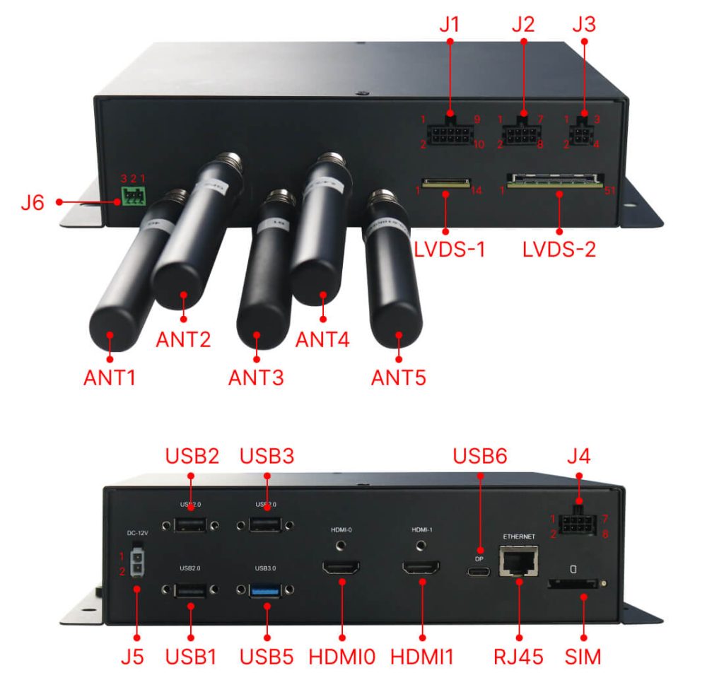
3.2 Product IO Interface Diagram
3.2.1 Interface Identification Diagram
dsgw 390 interface identification
dsgw 390 interface identification diagram
3.2.2 Interface definition
Serial number describe Remark
1 Fan connector Reserved core board cooling fan interface
2 Motherboard PCBA
3 Core board heat sink
4 PCBA of daughter board 1
5 PCBA of daughter board 2
K1 RECOVERY button
Not external, for debugging
K2 MASKROM button
K3 Hard reset button
J1 1 passive digital input, 3 digital outputs, 1 NTC temperature sensor input detection and 2 PWM outputs 1 passive digital input is isolated, 3 digital outputs are open collector outputs, 1 PWM interface is open collector output
J2 1 485 interface and 3 high-speed CAN interfaces, the maximum rate of CAN interface is 1Mbps The 485 interface is non-isolated, and the 3-way CAN interface is independently isolated
J3 2-way speaker output, speaker 8 ohm/3W 1 speaker for each left and right channel
J4 2 passive digital inputs, 2 digital outputs and 1 NTC temperature sensor input detection The 2 passive digital inputs are isolated and the 2 digital outputs are open collector outputs.
J5 Battery power supply interface, voltage range 9V to 12V
J6 Debug interface 1 UART interface, CMOS level, level 3.3V, 2.54mm pitch, 3Pin socket
LVDS-2 LVDS screen interface, 2 groups of LVDS interfaces, 4 pairs of signal lines in each group One 51-pin socket for external use
LVDS screen touch interface, USB2.0 HOST interface
LVDS-1 LVDS screen backlight driver interface, using PWM to drive the screen brightness One 14-pin socket for external use
LVDS screen temperature detection interface, using NTC temperature sensor to measure the screen temperature
ANT1 LTE 4G Main Antenna These three antennas are derived from the LTE 4G CAT4 module, module model EC20CEFILG-128-SGNS, Quectel Communications
ANT2 LTE 4G GPS Antenna
ANT3 LTE 4G Diversity Antenna
ANT4 WIFI&BT integrated antenna
ANT5 Lora Antenna
USB1 USB2.0 HOST interface
USB2 USB2.0 HOST interface
USB3 USB2.0 HOST interface
USB5 USB3.0 HOST interface
USB6 DP screen interface, multiplexed with the firmware burning interface External use Type C female connector
HDMI0 Connect HDMI display 0
HDMI1 Connect HDMI display 1
RJ45 10/100/1000Mbps Ethernet interface
SIM LTE 4G SIM card interface Micro-SIM card slot,Supports China Mobile, China Telecom and China Unicom
3.2.3 Interface Usage Description
3.2.3.1 Instructions for use of core board interface

The mainboard uses the RK3588J core board. The position of the core board on the PCBA is shown in the figure below:
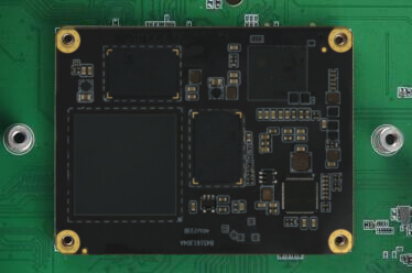
dsgw 390 instructions for use of core board interface

The four corners in the above picture are the four columns for fixing the core board. The size parameter is M2*3.0, and the corresponding fixing screw size can be M3*6.0mm.
The core board used on this PCBA has a RAM capacity of 8GB and an EMMC capacity of 64GB.

3.2.3.2 Fan Interface Instructions

The pin sequence of the core board cooling fan interface CON2 on the PCBA is shown in the figure below:

dsgw 390 fan interface instructions
Serial number Pin Name Pin Description IO level Remark
1 VCC_12V_FAN
Fan power supply
12V Fan power supply
2 FAN_FG Fan speed feedback signal 3.3V This signal can detect the fan speed
3 FAN_PWM Fan speed PWM control signal 5V The fan speed is controlled by this PWM signal
4 GND Signal Ground 0V

This interface is reserved. Whether to add a fan depends on the actual application.
The specifications of the fan socket CON2 are shown in the figure below:

dsgk 070 specifications of the fan socket
3.2.3.3 Fan Interface Instructions
The positions of the three buttons on the motherboard on the PCBA are shown in the figure below:
dsgw 390 positions of the three buttons

K1 is the RECOVERY button, K2 is the MASKROM button, and K3 is the hard reset button.
①RECOVERY button
Press the RECOVERY button, the system enters the RECOVERY state, under the premise that no button action is performed and the system has been burned with firmware, power on and enter the system directly; if the RECOVERY mode button is pressed when the system starts, RK3588 enters the Loader burning mode, when the PC recognizes the USB device, release the RECOVERY button to burn the firmware.
②MASKROM button
MASKROM is a dedicated pin for BOOT configuration, which determines the system startup sequence. This pin cannot be used for other functions. Press the MASKROM button, power on the core board again or press the reset button to put the device into the MASKROM state.
③Hard reset button
The hard reset button signal is connected to the hardware reset pin of the core board. Press this button and the core board will reset and restart.

3.2.3.4 J1 connector interface instructions
①The pin sequence of the J1 connector is shown in the figure below:
dsgw 390 j1 connector interface
Serial number Pin Name Pin Description IO level Remark
1 Digital input DI1+ Passive digital input positive VCC5V0_SYS_ISO1 Connect the manual/automatic switch button. This signal is isolated from the system ground and signal.
2 Digital input DI1- Passive digital input negative 0V
3 Digital output DO1+ Control KL87 relay to close and open single-side control, low-side drive 12V Open collector output, external relay model AP24512ABDNil60, Ningbo Puzheng Auto Parts Co., Ltd., the power supply of the relay coil is the same as the input power supply of the system, the power supply voltage is 9 to 16V, the control pin is high level, the relay is energized, otherwise, it is disconnected
4 Digital output DO2+ Control thermal management relay unilateral control, low side drive 12V
5 Digital output DO3+ Control KL15 relay unilateral control, low side drive 12V
6 null
7 Analog input AI1+ Vehicle thermal management, connected to NTC thermistor
8 Analog input AI1-
9 PWM output P1+, The collector has a 1.5K pull-up resistor output Vehicle thermal management, control cooling system-fan power supply ground
10 PWM output P2+, Open collector output Vehicle thermal management control cooling system-water pump power supply ground
②J1 board connector model: C3030WR-2x5P-G, brand: CJT, parameters are as follows:
dsgw 390 c3030wr 2x5p g

③The line connector model corresponding to the J1 board connector is: C3030HF-2x5P, brand: CJT, parameters are as follows:

dsgw 390 line connector model
3.2.3.5 J2 connector interface instructions
①The pin sequence of the J2 connector is shown in the figure below:
dsgw 390 pin sequence of the j2
Serial number Pin Name Pin Description IO level Remark
1 CAN0_H CAN1: Chassis CAN
500kbps, no terminal resistor, reserved position
High-speed CAN interface, the 3-way CAN interface is isolated from each other, and the 3-way CAN interface is also isolated from the system ground
2 CAN0_L
3 CAN1_H CAN2: Total CAN
500kbps, connected to 120 ohm terminal resistor
4 CAN1_L
5 CAN2_H CAN3: Discharge CAN
250kbps, no terminal resistor, reserved position
6 CAN2_L
7 RS485-A Connect to the lighting control board, the rate is 9600bps Non-isolated RS485 interface, shared ground with system ground
8 RS485-B

②J2 board connector model: C3030WR-2x4P-G, brand: CJT, parameters are as follows:

dsgw 390 c3030wr 2x5p g

③The line-end connector model corresponding to the J2 board-end connector is: C3030HF-2x4P, brand: CJT, and the parameters are as follows:

dsgw 390 line connector model
3.2.3.6 J3 connector interface instructions

①The pin sequence of the J3 connector is shown in the figure below:

dsgw 390 pin sequence of the j3
Serial number Pin Name Pin Description IO level Remark
1 SPEAK1-P Left channel speaker 1 output positive Speaker 8 ohm/3W
2 SPEAK1-N Left channel speaker 1 output negative
3 SPEAK2-P Right channel speaker 2 output positive
4 SPEAK2-N Right channel speaker 2 output negative

②J3 board connector model: C3030WR-2x2P-G, brand: CJT, parameters are as follows:

dsgw 390 c3030wr 2x5p g

③The line-end connector model corresponding to the J3 board-end connector is C3030HF-2x2P, and the parameters are as follows:

dsgw 390 line connector model
3.2.3.7 J4 connector interface instructions

①The pin sequence of the J4 connector is shown in the figure below:

dsgw 390 pin sequence of the j4
Serial number Pin Name Pin Description IO level Remark
1 Digital input DI2+ Passive digital quantity 2 input positive VCC5V0_SYS_ISO1 Connect the manual/automatic switch button. This signal is isolated from the system ground and signal.
2 Digital input DI2- Passive digital quantity 2 input negative 0V
3 Digital input DI3+ Passive digital quantity 3 input positive VCC5V0_SYS_ISO1
4 Digital input DI3- Passive digital quantity 3 input negative 0V
5 Digital output DO4+ Control KL15 relay unilateral control, low side drive Open collector output, external relay model AP24512ABDNil60, Ningbo Puzheng Auto Parts Co., Ltd., the power supply of the relay coil is the same as the input power supply of the system, the power supply voltage is 9 to 16V, the control pin is high level, the relay is energized, otherwise, it is disconnected
6 Digital output DO4+
7 Analog Input AI2+ Reserved for vehicle thermal management, connected to NTC thermistor
8 Analog input AI2 -
②J4 board connector model: C3030WR-2x4P-G, brand: CJT, parameters are as follows:
dsgw 390 c3030wr 2x5p g

③The line-end connector model corresponding to the J4 board-end connector is C3030HF-2x4P, and the parameters are as follows:

dsgw 390 line connector model
3.2.3.8 J5 connector interface instructions

①The pin sequence of the J5 connector is shown in the figure below:

dsgw 390 pin sequence of the j5
Serial number Pin Name Pin Description IO level Remark
1 VCC System input power positive pole Battery powered, voltage range 9V to 12V, 60W
2 GND System input power positive pole 0V

②J5 board connector model: C4201WR-2x1P, brand: CJT, parameters are as follows:

dsgw 390 c3030wr 2x5p g

③The line-end connector model corresponding to the J5 board-end connector is: C4201HF-2x1P, brand: CJT, and the parameters are as follows:

dsgw 390 line connector model
3.2.3.9 J6 connector interface instructions

①The pin sequence of the J6 connector is shown in the figure below:

dsgw 390 pin sequence of the j6
Serial number Pin Name Pin Description IO level Remark
1 DEBUG_RXD UART receiving signal 3.3V
UART signal is CMOS level
2 DEBUG_TXD UART sends signal 3.3V
3 GND Signal Ground
0V

②J6 board connector model: WJ15EDGRC-2.54-3P-1YY-00A, brand: Hangzhou Wanjie Electronics Co., Ltd., parameters are as follows:

dsgw 390 j6 board connector

③The line-end connector model corresponding to the J6 board-end connector is: WJ15EDGK-2.54-1P-1YY-00A, brand: Hangzhou Wanjie Electronics Co., Ltd., parameters are as follows:

dsgw 390 j6 board end connector
3.2.3.10 USB interface instructions

The USB interface is arranged as shown in the following figure:

dsgw 390 usb interface instructions
Serial number Pin Name Pin Description IO level Remark
USB1 USB2.0 HOST interface Chassis CUB2 USB port Maximum external output current 567mA
USB2 USB2.0 HOST interface External RGBD camera Maximum external output current 567mA
USB3 USB2.0 HOST interface Maximum external output current 567mA
USB5 USB3.0 HOST interface, reserved Reserved interface Maximum external output current 1000mA
3.2.3.11 HDMI Interface Instructions

The positions of HDMI0 and HDMI1 interfaces are shown in the following figure:

dsgw 390 hdmi interface instructions
Serial number Pin Name Pin Description IO level Remark
HDMI0 HDMI0 interface Display and sound output interface External Type A interface, external advertising screen, reserved
HDMI1 HDMI1 port Display and sound output interface
3.2.3.12 DP screen interface instructions

The position layout of the DP screen interface is shown in the following figure:

dsgw 390 dp screen interface
USB6 is Type-C interface, used for DP display function. Reserved for connecting Type-C screen and touch screen.
3.2.3.13 RJ45 interface instructions

The position of the RJ45 interface is shown in the following figure:

dsgw 390 rj45 screen interface
RJ45 is an Ethernet interface that supports 10M/100M/1000Mbps rates.
3.2.3.14 SIM interface instructions

The location of the SIM interface is shown in the following figure:

dsgw 390 sim screen interface
The above is the installation location of the LTE 4G SIM card.Micro-SIM card slot,Supports three major operators: China Mobile, China Telecom and China Unicom. SIM card holder model: SIM-212SA-KT-A2, brand: Dongguan Hanbo Electronic Technology Co., Ltd., specifications are shown in the figure below:
dsgw 390 sim card holder model
3.2.3.15 LVDS touch screen interface instructions

The LVDS touch display uses two interfaces, one is a 14-pin LVDS-1 interface and the other is a 51-pin LVDS-2 interface.

3.2.3.15.1 LVDS-1 Interface Usage Instructions

①The pin sequence of the LVDS-1 interface connector is shown in the figure below:

dsgw 390 lvds 1 interface
Serial number Pin Name Pin Description IO level Remark
1 LVDS_GND 0V
2 LEDK4 Backlight 4th LED cathode Each string has 8 LED lights connected in series, the typical current of each string is 95mA, and the maximum current is 100mA
3 LEDK3 Backlight 3rd LED cathode
4 LEDK2 Backlight 2nd LED cathode
5 LEDK1 Backlight 1st LED cathode
6 LVDS_GND 0V
7 LEDA Backlight 4 strings LED anode Typical 24V, maximum 27V
8 LEDA
9 LVDS_GND 0V
10 NCT_K NTC Thermistors Resistor model: NCP15XH103F0SRB
11 NCT_A
12 LVDS_GND 0V
13 VCC5V0_TP Screen touch panel output 5V power supply 5V External current limit 200mA
14 LVDS_GND 0V
dsgw 390 figure below

②LVDS-1 board-side connector model: A1004WR-S-14P-G, brand: CJT, parameters are as follows:

dsgw 390 lvds 1 board side connector model

③The line-end connector model corresponding to the LVDS-1 board-end connector is: A1004H-14P, brand: CJT, and the parameters are as follows:

dsgw 390 line end connector model
3.2.3.15.2 LVDS-2 Interface Instructions
①The pin sequence of the LVDS-2 interface connector is shown in the figure below:
dsgw 390 lvds 2 interface
Serial number Pin Name Pin Description IO level Remark
1 LVDS_GND 0V
2 VCC 3.3V Display screen power supply
3 VCC 3.3V
4 VOTP OTP power input 3.3V Not use: connect to
VCC
5 LVDS_GND 0V
6 LVDS_GND 0V
7 USB_DP USB2.0 data signal+ Single-ended impedance 50Ω, differential impedance 90Ω, connected to the display touch panel
8 USB_DM USB2.0 data signal -
9 LVDS_GND 0V
10 FAULT Abnormal status detection pin Normal: low
Abnormal : high
11 UPND Display vertical direction selection pin Image
12 SHLR Display horizontal direction selection pin
13 CSB Chip select pin Reserve
14 SDA I2C Interface Reserve
15 SCL
16 STBYB Standby mode setting pin Low level is effective
17 LVDS_GND
18 RESET Hard reset pin, Low level is effective
19 BIST BIST function enable pin, Normal: L; BIST: H
20 LVDS_GND 0V
21 LVDS_GND 0V
22 ELV3P LVDS even data output 3+ Single-ended impedance 50Ω, differential impedance 100Ω
23 ELV3N LVDS even data output 3-
24 LVDS_GND 0V
25 ELVCKP LVDS even clock output + Single-ended impedance 50Ω, differential impedance 100Ω
26 ELVCKN LVDS even clock output -
27 LVDS_GND 0V
28 ELV2P LVDS even data output 2+ Single-ended impedance 50Ω, differential impedance 100Ω
29 ELV2N LVDS even data output 2-
30 LVDS_GND 0V
31 ELV1P LVDS even data output 1+ Single-ended impedance 50Ω, differential impedance 100Ω
32 ELV1N LVDS even data output 1-
33 LVDS_GND 0V
34 ELV0P LVDS even data output 0+ Single-ended impedance 50Ω, differential impedance 100Ω
35 ELV0N LVDS even data output 0-
36 LVDS_GND 0V
37 OLV3P LVDS odd data output 3+ Single-ended impedance 50Ω, differential impedance 100Ω
38 OLV3N LVDS odd data output 3-
39 LVDS_GND 0V
40 OLVCKP LVDS odd clock output + Single-ended impedance 50Ω, differential impedance 100Ω
41 OLVCKN LVDS odd clock output -
42 LVDS_GND 0V
43 OLV2P LVDS odd data output 2+ Single-ended impedance 50Ω, differential impedance 100Ω
44 OLV2N LVDS odd data output 2-
45 LVDS_GND 0V
46 OLV1P LVDS odd data output 1+ Single-ended impedance 50Ω, differential impedance 100Ω
47 OLV1N LVDS odd data output 1-
48 LVDS_GND 0V
49 OLV0P LVDS odd data output 0+ Single-ended impedance 50Ω, differential impedance 100Ω
50 OLV0N LVDS odd data output 0-
51 LVDS_GND 0V
②LVDS-2 board connector model: LVDS-51P-3.75H, brand: Shenzhen Xingzhao Confidential Co., Ltd., parameters are as follows:
dsgw 390 lvds 2 board side connector model
③The line connector model corresponding to the LVDS-2 board connector: LVDS-2 adapter cable (34AWG&40AWG coaxial cable), the parameters are as follows:
dsgw 390 lvds 2 adapter cable

③LVDS screen model:COG-VLBJT195-01, Brand: BOE, parameters are as follows:

Parameter Specification Unit Remarks
Active area 292.032(H)x 109.512(V) mm 8:03
Number of pixels 1920(H) x RGB x720(V) pixels
Pixel pitch 0.1521(H) x0.1521 (V) mm
Pixel arrangement RGB horizontal stripe
Display colors 16.7M colors
Color gamut 72% % TyP.
Display mode Normally black
Module outline 301.632(W)x 124.812(H)x6.8(D) mm Without FPC&PCB&Component and EMI Tape
Viewing Direction(Human Eye) U/D/L/R Min 80/80/80/80 Typ 88/88/88/88

Table 2-1 Environment Absolute Maximum Ratings

Parameter Symbol Min. Max. Unit Remarks
LCD Logic Voltage DVDD 4 V Ta=25+1-20℃
Operating Temperature(Humidity) TOP -30 +85
RH 90 % At 60℃
Storage Temperature(Humidity) TST -40 +90
RH 90 % At 600℃

Table 3-3Electrical Specifications                         Ta=25+/-2℃

Parameter Symbol Values Unit Remark
Min TyP. Max
TFT Logic Power Voltage DVDD 3.0 3.3 3.6 V
Current IDVDD 300 550 mA
Input High Voltage Voltage VIH 0.7*VCC VCC V
Input Low Voltage Voltage VIL 0 0.3*VCC V
Supply current of LED backlight Per string 95 100 mA 8 LED
Total Supply current of LED Backlight ILEDTotal 380 400 mA 4 strings
Supply voltage of LED backlight Per string 24 27 V 4 strings
LED Power consumption of Total 9.12 10.8 W Note2

Table 3-5 LVDS AC Characteristics

Parameter Symbol Value Unit
Min. TyP. Max.
Clock frequency RXFCLK 20 95 MHZ
1 data bit time UI 1/7 TLVCYC
Clock high time TLVCH 4/(7*RXFCLK) UI
Clock low time TLVCL 3/(7*RXFCLK) UI
Position 1 TPOS1 -0.2 0 0.2 UI
Position 0 TPOS0 0.8 1 1.2 UI
Position 6 TPOS6 1.8 2 2.2 UI
Position 5 TPOS5 2.8 3 3.2 UI
Position 4 TPOS4 3.8 4 4.2 UI
Position 3 TPOS3 4.8 5 5.2 UI
Position 2 TPOS2 5.8 6 6.2 UI
Input eye width TEYEW 0.6 UI
Input eye border TEX 0.2 UI
LVDS wake up time TENLVDS 150 us

Table 3-6 LVDS DC Characteristics

Parameter Symbol Spec. Unit Condition
Min. TyP. Max.
Differential input common modevoltage Vcm |Vid|/2 VDD-1.2-|vid|/2 V
LVDS input voltage range(signaled-end) Vinlv 0 VDD-1.2 V
Differential input voltage |vid| 0.1 0.6 V
Differential input leakage Current |RVXliz| -10 +10 uA
3.2.3.16 Antenna Interface Instructions

①The positions of the five external antennas are arranged as shown in the figure below:

dsgw 390 positions of the five external
Serial number Pin Name Corresponding antenna frequency range Remark
ANT1 LTE 4G Main Antenna 698-960MHZ and 1700-2700MHZ Module model EC20CEFILG-128-SGNS, Quectel Communications
ANT2 LTE 4G GPS Antenna 1555-1595MHZ
ANT3 LTE 4G Diversity Antenna 698-960MHZ and 1700-2700MHZ
ANT4 WIFI&BT integrated antenna 2400-2500MHZ and
5150-5850MHZ
Module model FCS950RACMD, Quectel Communications
ANT5 Lora Antenna 470-510MHZ Chip model LLCC68IMLTRT, SEMTECH

②The main technical parameters of LTE 4G main antenna ANT1 and LTE 4G diversity antenna ANT3 are shown in the following figure:

Main technical parameters
Frequency Range(MHZ) 698-960MHZ
1700-2700MHZ
Impedance(Ω) 50±10
Gain(dBi) 2.5±1
ReTumLoss(dB) ≤-8
VSWR ≤3.0
Polarization Linear Vertical
Connector Type BNC
Physical Properties
Antenna Base ABS
Operating Temp -20℃-+60℃
Storage Temp -20'C-+70℃

③The main technical parameters of LTE 4G GPS antenna ANT2 are shown in the figure below:

Main technical parameters
Frequency Range(MHZ) 1555-1595MHZ
Impedance(Ω) 50±10
Gain(dBi) 1.5±0.5
ReTumLoss(dB) ≤-10
VSWR ≤2.0
Polarization Linear Vertical
Connector Type BNC
Physical Properties
Antenna Base ABS
Operating Temp -20℃-+60℃
Storage Temp -20'C-+70℃

④The main technical parameters of WIFI&BT integrated antenna ANT4 are shown in the figure below:

Main technical parameters
Frequency Range(MHZ) 2400-2500MHZ
5150-5850MHZ
Impedance(Ω) 50±10
Gain(dBi) 3±0.5
ReTumLoss(dB) ≤-10
VSWR ≤2.0
Polarization Linear Vertical
Connector Type BNC
Physical Properties
Antenna Base ABS
Operating Temp -20℃-+60℃
Storage Temp -20'C-+70℃

⑤The main technical parameters of Lora antenna ANT5 are shown in the figure below:

Main technical parameters
Frequency Range(MHZ) 470-510MHZ
Impedance(Ω) 50±10
Gain(dBi) 0.5±0.5
ReTumLoss(dB) ≤-10
VSWR ≤2.5
Polarization Linear Vertical
Connector Type BNC
Physical Properties
Antenna Base ABS
Operating Temp -20℃-+60℃
Storage Temp -20'C-+70℃
3.3 Status indicator light description

none

4. Software Instructions

4.1 Mainboard buttons and interface description
4.1.1 Button Description
Serial number interface illustrate
1 recovery Press and hold the power on system to enter the loader burning mode
2 RESET Restart
3 MASKROM Press and hold the store system to enter the MASKROM burning mode
4.1.2 Interface Description

NA

4.2 Debug serial port parameter settings

It is recommended to use MobaXterm to access, the recommended download address is: https://mobaxterm.mobatek.net/download-home-edition.html
The effect after the tool opens the serial port is as follows:

dsgw 390 debug serial port
4.2.2 Serial port settings

l Debug serial port baud rate 1500000
18 data bits
1 stop bit
No verification
No flow control
Please note that there is no 1500000 in the serial port baud rate drop-down box. You need to enter it directly.
See the figure below for details

dsgw 390 serial port settings
4.2.3 Serial port connection diagram
dsgw 390 serial port connection diagram
4.3 Firmware Burning
4.3.1 Preparation
Prepare the Materials illustrate
Burning PC Windows 7 and above
RKDevTool v2.93 and above
USB type C cable
4.3.2 SDK application and download
4.3.2.1 Apply for SDK
sdk application process

The SDK versions of different Dusun chip platforms need to be applied to the corresponding business end respectively. For example, your company has received the SDK for RK3288, and now there is a new project that requires the SDK for RK3588. We need to contact the corresponding business end of Dusun for business confirmation, and the business end will assist in the application. After approval by Dusun auditors, the technical department can disclose information to your company.
Notice:
The SDK code management released by Dusun follows Google’s REPO method. Users are not recommended to delete the SDK’s REPO and GIT version records.

4.3.2.2 Generate server key

Enter on the server command line

				
					ssh-keygen -t rsa -C " xxxx@xxxx.com "


Keep pressing Enter and do not enter the task characters;
After generating the key, email the ~/.ssh/id_rsa.pub file to Dusun

dsgw 390 generate server key
4.3.2.3 Git Configuration

Enter on the server command line

				
					git config --global user.email " You@example.com "
git config --global user.name "Your Name"
				
			
4.3.2.4 SDK Download

Download the repo

				
					git clone ssh:// git@roombanker.x3322.net :2223/dusun_repo.git


Add environment variables

				
					sudo cp -f ~/work/dusun_repo/repo /usr/bin/repo
sudo chmod +x /usr/bin/repo


Get the code

				
					mkdir -p ~/work/project/dev
cd ~/work/project/dev
repo init -u ssh:// git@roombanker.x3322.net :2223/rk3588_linux_rt/manifests_first.git -m rk3588_linux.xml -b dev --no-repo-verify
repo sync -c -j8
repo start master --all
				
			
4.3.3 Download the burning software tool
4.3.3.1 Download PC flash tool

Flashing tool link, the installation package is located below the source code library

				
					tools/windows/RKDevTool_Release_v3.31.zip
				
			
4.3.3.2. PC driver download

The computer needs to install the adb USB driver, the installation package is located below the source code library

				
					tools/windows/DriverAssitant_v5.13.zip
				
			
4.3.4 Solid Zen Dao Burning
4.3.4.1 Flash connection diagram
dsgw 390 flash connection diagram
4.3.4.2 Flashing steps
  1. Connect the development board typec to the computer, open RKTool, and install the tool driver
  2. Press and hold the recovery/MASKROM/USB_KET button, then power on.
  3. Start burning
dsgw 390 flashing steps
4.4 SDK Introduction
4.4.1. Compile Commands
				
					#Compile all
RK_ROOTFS_SYSTEM=debian ./build.sh  
# Compile kernel separately
RK_ROOTFS_SYSTEM=debian ./build.sh kernel
				
			
4.4.2 Compilation Products

Use update.img for the flash package to generate the firmware location

				
					output/update/Image/update.img
				
			
4.4.3 Commonly used interfaces
4.4.3.1 Wifi

Run “ds_conf_ap.sh”, the script starts the Wi-Fi AP.
SSID: “dsap”. PWD: “12345678”

				
					#ds_conf_ap.sh
192.168.10.1
start hostapd
Configuration file: /etc/hostapd.conf
wlan0: interface state UNINITIALIZED->COUNTRY_UPDATE
start dnsmasq
Stopping dnsmasq: OK
Starting dnsmasq: OK Done!!!!!!
#
#
# iwconfig
lo	no wireless extensions.

wlan0 IEEE 802.11an ESSID:"dsap" Nickname:"<WIFI@REALTEK>"        
    Mode:Master Frequency:5.745 GHz Access Point: 20:57:9E:8B:70:F5
    Bit Rate:72.2 Mb/s Sensitivity:0/0
    Retry:off RTS thr:off Fragment thr:off
    Encryption key:off
    Power Management:off
    Link Quality=1/100 Signal level=1/100 Noise level=0/100
    Rx invalid nwid:0 Rx invalid crypt:0 Rx invalid frag:0
    Tx excessive retries:0 Invalid misc:0 Missed beacon:0
eth0	no wireless extensions.
#
# ifconfig
eth0	Link encap:Ethernet HWaddr 0A:11:D3:88:1E:B5
    inet addr:192.168.1.4 Bcast:192.168.1.255 Mask:255.255.255.0
    inet6 addr: fe80::811:d3ff:fe88:1eb5/64 Scope:Link
    UP BROADCAST RUNNING MULTICAST MTU:1500 Metric:1
    RX packets:73386 errors:0 dropped:0 overruns:0 frame:0
    TX packets:52722 errors:0 dropped:0 overruns:0 carrier:0    
    collisions:0 txqueuelen:1000
    RX bytes:64535523 (61.5 MiB) TX bytes:4975499 (4.7 MiB)
    Interrupt:40

lo	Link encap:Local Loopback
    inet addr:127.0.0.1 Mask:255.0.0.0
    inet6 addr: ::1/128 Scope:Host
    UP LOOPBACK RUNNING MTU:65536 Metric:1
				
			
4.4.3.2 Ethernet
				
					root@DUSUN:~# ifconfig eth0
    eth0: flags=4163<UP,BROADCAST,RUNNING,MULTICAST> mtu 1500
    inet 192.168.124.22 netmask 255.255.255.0broadcast 192.168.124.255
    inet6 fe80::fcef:8eff:fe73:7e62 prefixlen 64 scopeid 0x20<link>
    ether fe:ef:8e:73:7e:62 txqueuelen 1000(Ethernet)
    RX packets 252 bytes 71409 (71.4 KB)
    RX errors 0 dropped 0 overruns 0 frame 0
    TX packets 278 bytes 42041 (42.0 KB)
    TX errors 0 dropped 0 overruns 0 carrier 0 collisions 0
    device interrupt 80
				
			
4.4.3.3 LTE

Run bg96_dial.sh

				
					# ifconfig eth0 down
#
# bg96_dial.sh

AT+CPIN?
+CPIN: READY
OK AT+CSQ
+CSQ: 31,99

OK

sent [IPCP ConfAck id=0x1]
rcvd [IPCP ConfNak id=0x3 <addr 172.28.36.150> <ms-dns1 221.131.143.69> <ms-dns2 112.4.0.55>]
sent [IPCP ConfReq id=0x4 <addr 172.28.36.150> <ms-dns1 221.131.143.69> <ms-dns2 112.4.0.55>]
rcvd [IPCP ConfAck id=0x4 <addr 172.28.36.150> <ms-dns1 221.131.143.69> <ms-dns2 112.4.0.55>]
Could not determine remote IP address: defaulting to 10.64.64.64 local IP address 172.28.36.150
remote IP address 10.64.64.64 primary   
DNS address 221.131.143.69
secondary DNS address 112.4.0.55<===== after connected,type Ctrl+Z

^Z[1]+ Stopped    bg96_dial.sh
#
# ifconfig
    lo	Link encap:Local Loopback
    inet addr:127.0.0.1 Mask:255.0.0.0
    inet6 addr: ::1/128 Scope:Host
    UP LOOPBACK RUNNING MTU:65536 Metric:1
    RX packets:131 errors:0 dropped:0 overruns:0 frame:0
    TX packets:131 errors:0 dropped:0 overruns:0 carrier:0
    collisions:0 txqueuelen:1
    RX bytes:12350 (12.0 KiB) TX bytes:12350 (12.0 KiB)

ppp0	Link encap:Point-to-Point Protocol
    inet addr:172.28.36.150 PtP:10.64.64.64 Mask:255.255.255.255
    UP POINTOPOINT RUNNING NOARP MULTICAST MTU:1500 Metric:1
    RX packets:6 errors:0 dropped:0 overruns:0 frame:0
    TX packets:6 errors:0 dropped:0 overruns:0 carrier:0
    collisions:0 txqueuelen:3
    RX bytes:96 (96.0 B) TX bytes:114 (114.0 B)
    
wlan0 Link encap:Ethernet HWaddr 20:57:9E:8B:70:F5
    inet addr:192.168.10.1 Bcast:0.0.0.0 Mask:255.255.255.0
    inet6 addr: fe80::2257:9eff:fe8b:70f5/64 Scope:Link
    UP BROADCAST RUNNING MULTICAST MTU:1500 Metric:1
    RX packets:33387 errors:0 dropped:0 overruns:0 frame:0  
    TX packets:56331 errors:0 dropped:636 overruns:0 carrier:0    
    collisions:0 txqueuelen:1000
    RX bytes:5077398 (4.8 MiB) TX bytes:78164665 (74.5 MiB)
#
# ping www.baidu.com
PING www.baidu.com (36.152.44.96): 56 data bytes
64 bytes from 36.152.44.96: seq=0 ttl=56 time=317.025 ms
				
			
4.4.3.4 Button
				
					#enter
dig_in1: cat /sys/class/gpio/gpio153/value (the value will change when the key is pressed)
dig_in2: cat /sys/class/gpio/gpio508/value (the value will change when the key is pressed)
dig_in3: cat /sys/class/gpio/gpio507/value (the value will change when the key is pressed)
#Output
dig_out1: echo 1 > /sys/class/gpio/gpio122/value (output high level)
	      echo 0 > /sys/class/gpio/gpio122/value (output low level)
dig_out2: echo 1 > /sys/class/gpio/gpio102/value (output high level)
	      echo 0 > /sys/class/gpio/gpio102/value (output low level)
dig_out3: echo 1 > /sys/class/gpio/gpio131/value (output high level)
	      echo 0 > /sys/class/gpio/gpio131/value (output low level)
dig_out4: echo 1 > /sys/class/gpio/gpio112/value (output high level)
	      echo 0 > /sys/class/gpio/gpio112/value (output low level)
dig_out5: echo 1 > /sys/class/gpio/gpio124/value (output high level)
	      echo 0 > /sys/class/gpio/gpio124/value (output low level)
				
			
4.4.3.5 Audio
				
					root@DUSUN:~# aplay /path/audio file

#Volume adjustment command
alsamixer

#Amplifier
aw87565
				
			
4.4.3.6 485

458 port name, /dev/ttyS5

4.4.3.7 ADC
				
					#temp_ntc2
cat /sys/bus/iio/devices/iio\:device0/in_voltage_raw  
#temp_ntc1
cat /sys/bus/iio/devices/iio\:device0/in_voltage_raw  
#power、display
cat /sys/bus/iio/devices/iio\:device2/in_voltage* 
				
			
4.4.3.8 PWM
				
					#fan
echo 0 > /sys/class/pwm/pwmchip1/export   
echo 1000000 > /sys/class/pwm/pwmchip1/pwm0/period
echo 500000 > /sys/class/pwm/pwmchip1/pwm0/duty_cycle
echo 1 > /sys/class/pwm/pwmchip1/pwm0/enable

#Water Pump
echo 0 > /sys/class/pwm/pwmchip2/export   
echo 1000000 > /sys/class/pwm/pwmchip2/pwm0/period
echo 500000 > /sys/class/pwm/pwmchip2/pwm0/duty_cycle
echo 1 > /sys/class/pwm/pwmchip2/pwm0/enable
				
			
4.4.3.9 CAN
				
					#ifconfig can0 down

#Configure CAN frequency 500khz
#ip link set can0 type can bitrate 500000 loopback off
#ip link set can0 up

#View the can node information after configuration;
#ip -details link show can0  

#canreceive
#./candump can0 #Block receiving, print r if there is information received

#can send:
#./cansend can0 123#112233445566 #This test program sends a maximum of 8 bytes of data at a time;


5. Relevant standards and certifications

5.1 Hazardous Substance Standards
5.1.1 ROHS

Chinese Standard: GB/T 26572-2011
EU Standard: Directive 2011/65/EU
Remark:The components used in current products comply with ROHS standards

5.1.2 REACH

EU Standard: EU Regulation (EC) No 1907/2006 (REACH)
Remark:The components used in the current products comply with REACH standards

5.2 Anti-vibration standard STA-2A
5.2.1 Vibration Standards
1 Random vibration test 1. Place 3 noodles on the platform for 30 minutes.
2. Place Noodle 1 on the platform for 10 minutes.
3. Place side 2 or side 4 on the platform for 10 minutes.
4. Place surface 5 or 6 on the platform for 10 minutes.
5. Frequency: 1…4…100…200
6. PSD: 0.0001…0.01…0.01…0.0001
There is no obvious damage to the box after the random vibration test
2 Fixed displacement test Displacement: 25 mm
Displacement times: 14200 ci
There is no obvious damage to the box after the displacement test
3 Sinusoidal vibration test (packaging) Image 1. The appearance, function and performance of the equipment under test meet the specifications of the relevant standards without obvious changes, and the functions of the equipment meet the requirements of Table 2.
2. Minor surface damage (such as scratches, nicks, etc.) of the sample meets the requirements.
3. Some parts of the sample (such as connectors) are allowed to have slight deformation, but this deformation cannot affect the mechanical and electrical properties of the device.
4 Sinusoidal vibration test (bare metal)
Image
1. The appearance, function and performance of the equipment under test meet the specifications of the relevant standards without obvious changes, and the functions of the equipment meet the requirements of Table 2.
2. Minor surface damage (such as scratches, nicks, etc.) of the sample meets the requirements.
3. Some parts of the sample (such as connectors) are allowed to have slight deformation, but this deformation cannot affect the mechanical and electrical properties of the device.
5.2.2 Drop Standard
1 Package drop test 1. Wt< 10 Kg, drop 97 cm,
2. Wt:10 ~ 19 Kg, drop 81 cm,
3. 19 ~ 28 Kg, drop 66 cm,
4. Test standard: one corner, three sides, six faces, ten drops in total.Image
There is no obvious damage to the box after the drop test
2 Bare metal drop 1. Sample with normal function, no power supply
2. Drop mode: 6 sides, the drop sides are bottom, front, left, right, back and front in order;
3. Drop height
a) Excluding display screen and optical engine products
Free fall from a height of 100 cm onto a wooden floor no less than 3 cm thick
b) Products containing display screens and optical engines
Free fall from a height of 80cm onto a wooden floor no less than 3cm thick
1. The appearance, function and performance of the equipment under test meet the specifications of the relevant standards without obvious changes, and the functions of the equipment meet the requirements of Table 2.
2. Minor surface damage (such as scratches, nicks, etc.) of the sample meets the requirements.
3. Some parts of the sample (such as connectors) are allowed to have slight deformation, but this deformation cannot affect the mechanical and electrical properties of the device.
3 Drop (Packaging) Image 1. The appearance, function and performance of the equipment under test meet the specifications of the relevant standards without obvious changes, and the functions of the equipment meet the requirements of Table 2.
2. Minor surface damage (such as scratches, nicks, etc.) of the sample meets the requirements.
3. Some parts of the sample (such as connectors) are allowed to have slight deformation, but this deformation cannot affect the mechanical and electrical properties of the device.
5.2.3 Impact standards
1 Impact test 1. Impact spectrum: half sine, duration: 11 milliseconds
2. Acceleration: 30m/s2, impact direction: 6 sides
3. Test duration: 6 sides, 3 impacts per side
1. Calculate the test pressure value x1.4
2. Calculation of test pressure
3. Test load
4. The appearance, function and performance of the equipment under test meet the specifications of the relevant standards without obvious changes, and the functions of the equipment meet the requirements of Table 2.
5. Minor surface damage (such as scratches, nicks, etc.) of the sample meets the requirements.
6. Some parts of the sample (such as connectors) are allowed to have slight deformation, but this deformation cannot affect the mechanical and electrical properties of the device.
5.3 EMC implementation standards

EU standards: EN55032:2015+A11:2020/EN55035:2017+A11:2020/ETSI EN 301489-1 V2.2.3(2019-11)/ETSI EN 301489-X
Chinese Standard: GB/T 26572-2011
Note: The current product is designed strictly in accordance with EMC standards

5.4 Authentication Support
5.3.1 Proxy Client Authentication

The customer only needs to provide the application company information, and Dongsheng will be responsible for all the certification processes
The certification process is shown in the following example (CE certification):

ce certificate
5.3.2 Customer Self-Authentication

① Dongsheng provides certification related materials, the list of materials is as follows (contact the project leader, who will coordinate and organize the materials):

  1. BOM list (all in English)
  2. Body Label
  3. Block diagram
  4. Parts placement
  5. PCB layout
  6. Schematic diagram SCH
  7. User manual
  8. Antenna Specifications
  9. List of key safety components (with safety component certificates, such as relays, fuses, terminal blocks, etc.)
  10. PCB-UL certificate

② Dongsheng provides certification technical support (fixed frequency, safety regulations, EMC)
Contact the project leader, who will coordinate with relevant technical personnel to provide technical support.

6. Order

6.1 Model Description

⚠️:Order sub-model and corresponding product description

Related IoT Product Specifications

DSGW-560 Oil storage explosion-proof gateway

DSGW-560 Oil storage explosion-proof gateway is designed based on the Rockchip RK3308J, specifically tailored for high reliability and high stability in oil depot data acquisition

DSGW-090-Caregiving Nursing Bed IoT Gateway

The DSGW-090-Caregiving gateway, featuring an MTK7628 CPU and OpenWrt support, is tailored for healthcare. With an RJ45 serial port and BLE compatibility, it connects seamlessly

Looking For An IoT Device Supplier For Your Projects?

CONTACT US

    This site is protected by reCAPTCHA and the Google Privacy Policy and Terms of Service apply.

    IoT Gateways for Recommendation

    CONTACT US

      This site is protected by reCAPTCHA and the Google Privacy Policy and Terms of Service apply.

      Welcome to DusunIoT

      Hi there 👋 Is there anything we can help you with today? Please fill in the form below for the team to follow up if you become disconnected.

        DusunIoT Distributor Program

          This site is protected by reCAPTCHA and the Google Privacy Policy and Terms of Service apply.

            This site is protected by reCAPTCHA and the Google Privacy Policy and Terms of Service apply.