1. Product Description of DSOM-130N NXP i.MX8M Plus SoM
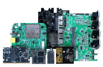
The i.MX 8M Plus SoM (System on Module) utilizes the NXP i.MX 8M Plus processor, featuring either a quad-core or dual-core Cortex-A53 CPU with a high-performance frequency of 1.6 GHz, along with a Cortex-M7 CPU operating at up to 800 MHz.
The NXP i.MX 8M Plus SoM series is designed for machine learning and vision, advanced multimedia, and reliable industrial automation, catering to the growing demands of smart homes, buildings, cities, and Industry 4.0 applications.
The DSOM-130N system on module offers a wide range of development documents and software resources that are both free and open-source. This convenience enables developers to enhance their efficiency and shorten the development cycle.
- Compact form factor with numerous GPIO interfaces
- Dimensions: 62mm x 36mm, featuring a board-to-board connector
- Equipped with an NPU with 2.3 TOPS
- Includes VPU, GPU, ISP, HiFi 4, and CAN-FD
- Dual Gb Ethernet support, one with Time Sensitive Networking (TSN) for gateway applications requiring low latency
- eMMC up to 16GB
- RAM up to 2GB
- 8-layer board-to-board connector, manufactured using immersion gold technology, includes an independent ground signal layer and lead-free
- Provides 320 PIN outputs, including nearly all CPU pins
- RoHS certified
- Industrial Control: Machine vision and robot controllers, building safety, power grid and distribution, industrial computers
- Smart City: Traffic detectors and traffic optimization, targeted advertising, visual payment systems
- Smart Home: Intelligent robots, appliances, AI home servers, and alarm centers
- Communication Infrastructure: Teleconferencing systems
2. System Block Diagram of DSOM-130N NXP i.MX8M Plus SoM
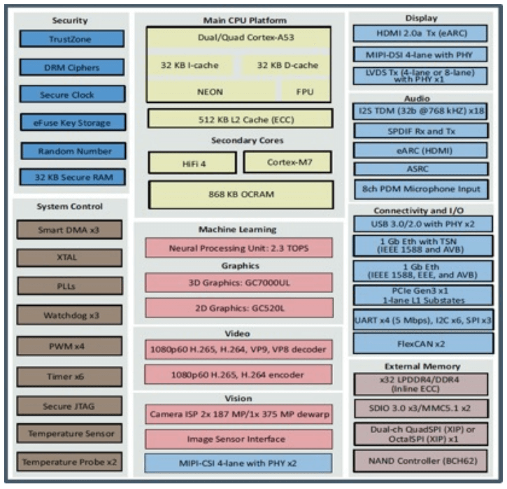
The compatible CPU models of the core board are shown in the table below, and our company has chosen the model of MIMX8ML8CVNKZAB.
For more information on i.MX8M Plus, please visit the NXP official website:
https://www.nxp.com.cn/products/ processors-and-microcontrollers/arm-processors/i-mx-applications-processors/i-mx-8-processors/i-mx-8m-plus-arm-cortex-a53-machine-learning-vision-multimedia- and-industrial-iot:IMX8MPLUS
| Part Number | Device Description | Part difference description | Number of A53 Cores | A53 speed | Temp Width |
|---|---|---|---|---|---|
| MIMX8ML8CVNKZAB | i.MX 8M Plus Quad | NPU,ISP, VPU, HiFi 4, CAN-FD | 4 | 1.6 GHz | Industrial |
| MIMX8ML6CVNKZAB | i.MX 8M Plus Quad | ISP, VPU, CAN-FD | 4 | 1.6 GHz | Industrial |
| MIMX8ML4CVNKZAB | i.MX 8M Plus QuadLite | CAN-FD | 4 | 1.6 GHz | Industrial |
| MIMX8ML3CVNKZAB | i.MX 8M Plus Dual | NPU,ISP, VPU, HiFi 4, CAN-FD | 2 | 1.6 GHz | Industrial |
| MIMX8ML8DVNLZAB | i.MX 8M Plus Quad | NPU,ISP, VPU, HiFi 4, CAN | 4 | 1.8 GHz | Consumer |
| MIMX8ML6DVNLZAB | i.MX 8M Plus Quad | ISP, VPU, CAN | 4 | 1.8 GHz | Consumer |
| MIMX8ML4DVNLZAB | i.MX 8M Plus QuadLite | CAN | 4 | 1.8 GHz | Consumer |
| MIMX8ML3DVNLZAB | i.MX 8M Plus Dual | NPU,ISP, VPU, HiFi 4, CAN | 2 | 1.8 GHz | Consumer |
3. Basic Parameters and Interfaces of DSOM-130N NXP i.MX8M Plus SoM
| Item | Parameter |
|---|---|
| CPU | Quad Cortex®-A53 processors operation up to 1.6 GHz Cortex®-M7 CPU operating up to 800 MHz |
| GPU | ● GC7000UL with OpenCL and Vulkan support ● 2 shaders ● 166 million triangles/sec ● 1.0 giga pixel/sec ● 16 GFLOPs 32-bit ● Supports OpenGL ES 1.1, 2.0, 3.0, OpenCL 1.2, Vulkan ● Core clock frequency of 1000 MHz ● Shader clock frequency of 1000 MHz ● GC520L for 2D acceleration ● Render target compatibility between 3D and 2D GPU (super tile status buffer) |
| VPU | Video Decode ● 1080p60 HEVC/H.265 Main, Main 10 (up to level 5.1) ● 1080p60 VP9 Profile 0, 2 ● 1080p60 VP8 ● 1080p60 AVC/H.264 Baseline, Main, High decoder Video Encode ● 1080p60 AVC/H.264 encoder ● 1080p60 HEVC/H.265 encoder |
| RAM | 2GB (1GB/4GB optional) |
| NPU | 2.3 TOP/s Neural Network performance ● Keyword detect, noise reduction, beamforming ● Speech recognition (i.e. Deep Speech 2) ● Image recognition (i.e. ResNet-50) |
| Storage | eMMC 16 GB (8GB / 16GB / 32GB eMMC optional) |
| Operating Voltage | Typical voltage 5V/2.5A |
| OS | Linux |
| Temperature | Operating Temperature: -40 °C ~80 °C |
| Storage Temperature: -40 °C ~85 °C | |
| Humidity | 10~95% (Non-condensing) |
| Barometric Pressure | 76Kpa ~106Kpa |
| Size | 62mm × 36mm × 4.0mm |
| Item | Parameter |
|---|---|
| USB 2.0 | 2 X USB2.0, two of which is for OTG |
| USB 3.0 | 2 X USB3.0,with intergrated PHY |
| PCIE | 2 X PCIE, Supports 1-way PCI Express Gen3.0 |
| MIPI CSI | 2 X MIPI CSI,Provide two 4-lane MIPI camera serial interfaces, capable of operating up to 1.5 Gbps |
| MIPI DSI | 1 X MIPI DSI,Provide 1 4-lane MIPI display serial interface, capable of operating up to 1.5 Gbps ● 1080 p60 ● WUXGA (1920x1200) at 60 Hz ● 1920x1440 at 60 Hz ● UWHD (2560x1080) at 60 Hz ● WQHD (2560x1440) by reduced blanking mode |
| HDMI | 1X HDMI ● Supports HDMI 2.0a display resolution up to 4Kp30 ● Supports HDMI2.1 eARC |
| LVDS | 1X LVDS, ● Single channel (4 lanes) support 720p60; ● Dual asynchronous channels (8 data, 2clocks) support 1920x1200p60 |
| Ethernet | 2 X RGMII, Supports two RGMII interfaces, with one supporting TSN |
| SDIO | 2 X SDIO ● SD2, 4-bit, supports 1.8/3.3V mode switching; ● SD1, 8-bit, only supports 1.8V mode |
| 4 X UART , The maximum supported baud rate is 4Mbp | |
| SPI | 3 X SPI , The maximum supported speed is 52Mbit/s, and the master-slave mode can be configured |
| I2C | 5 X I2C, The maximum speed supported in standard mode is 100Kbit/s; The maximum supported speed in fast mode is 400Kbit/s |
| CAN | 2 X CAN, The communication controller of CAN is implemented using the CAN FD protocol, as well as the CAN protocol that complies with the CAN 2.0B protocol specification. (CAN FD requires CPU version support) |
| SAI | 6 X SAI, Synchronous Audio Interface (SAI), a full duplex serial interface that supports frame synchronization, such as I2S, AC97, TDM, and codec/DSP interfaces |
| SPDIF | 1 X SPDIF,A standard audio file transfer format jointly developed by Sony and Philips |
| PWM | 4 X PWM,With 16 bit counter |
| QSPI | 1 X QSPI,Already occupied by the core board, connected to 16MB of No Flash |
| JTAG | 1 X JTAG,For debugging |
| Upgrade | supports local firmware upgrades via USB interface |
4. Pin Definition
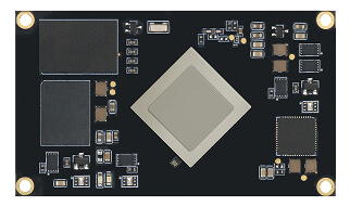
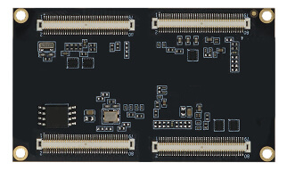
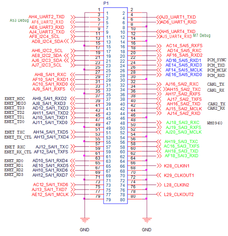
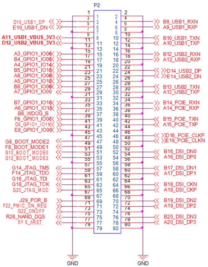
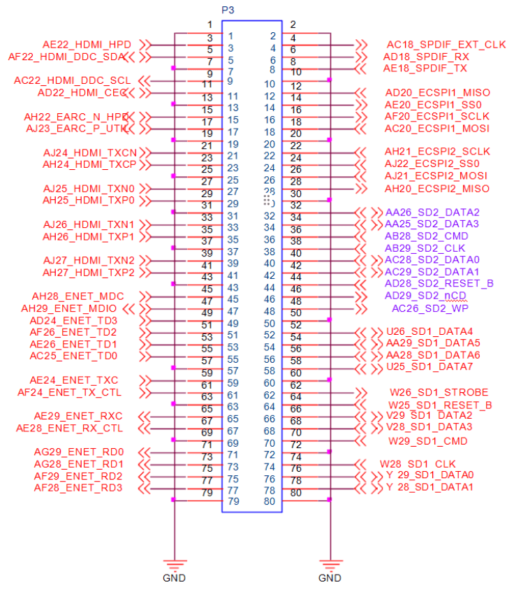
| NUM | Ball | Signal | GPIO | Vol | Spec | Default |
|---|---|---|---|---|---|---|
| LU_1 | — | GND | — | — | GND | GND |
| LU_3 | AH4 | UART2_TXD | GPIO5_IO25 | 3.3V | UART2(A53 debug) data sending | UART2_TXD |
| LU_5 | AF6 | UART2_TXD | GPIO5_IO24 | 3.3V | UART2(A53 debug) data receiving | UART2_RXD |
| LU_7 | AE6 | UART3_TXD | GPIO5_IO26 | 3.3V | UART3 data receiving | UART1_CTS |
| LU_9 | AJ4 | UART3_TXD | GPIO5_IO27 | 3.3V | UART3 data receiving | UART1_RTS |
| LU_11 | AF8 | I2C4_SCL | GPIO5_IO20 | 3.3V | I2C4 clock | I2C4_SCL |
| LU_13 | AD8 | I2C4_SDA | GPIO5_IO21 | 3.3V | I2C4 data | I2C4_SDA |
| LU_15 | — | GND | — | — | GND | GND |
| LU_17 | AH6 | I2C2_SCL | GPIO5_IO16 | 3.3V | I2C2 clock | I2C2_SCL |
| LU_19 | AE8 | I2C2_SDA | GPIO5_IO17 | 3.3V | I2C2 data | I2C2_SDA |
| LU_21 | AJ6 | I2C3_SDA | GPIO5_IO19 | 3.3V | I2C3 data | I2C3_SDA |
| LU_23 | AJ7 | I2C3_SCL | GPIO5_IO18 | 3.3V | I2C3 clock | I2C3_SCL |
| LU_25 | — | GND | — | — | GND | GND |
| LU_27 | AH8 | SAI1_RXC | GPIO4_IO1 | 1.8V | SAI1 receive bit clock | 4G_RST |
| LU_29 | AF10 | SAI1_RXD1 | GPIO4_IO3 | 1.8V | SAI1 receive data 1 | 5GPWR_RESE |
| LU_31 | AC10 | SAI1_RXD0 | GPIO4_IO2 | 1.8V | SAI1 receive data 0 | 5GPWR_ON/O |
| LU_33 | AJ9 | SAI1_RXFS | GPIO4_IO0 | 1.8V | SAI1 receive frame sync | 4G/5G_PWR |
| LU_35 | — | GND | — | — | GND | GND |
| LU_37 | AH9 | SAI1_RXD2 | GPIO4_IO4 | 1.8V | SAI1 receive data 2 | ENET1_MDC |
| LU_39 | AJ8 | SAI1_RXD3 | GPIO4_IO5 | 1.8V | SAI1 receivedata 3 | ENET1_MDIO |
| LU_41 | AD12 | SAI1_TXD3 | GPIO4_IO15 | 1.8V | SAI1 send data 3 | ENET1_TD3 |
| LU_43 | AH11 | SAI1_TXD2 | GPIO4_IO14 | 1.8V | SAI1 send data 2 | ENET1_TD2 |
| LU_45 | AJ10 | SAI1_TXD1 | GPIO4_IO13 | 1.8V | SAI1 send data 1 | ENET1_TD1 |
| LU_47 | AJ11 | SAI1_TXD0 | GPIO4_IO12 | 1.8V | SAI1 send data 0 | ENET1_TD0 |
| LU_49 | — | GND | — | — | GND | GND |
| LU_51 | AH14 | SAI1_TXD5 | GPIO4_IO17 | 1.8V | SAI1 send data 5 | ENET1_TXC |
| LU_53 | AH13 | SAI1_TXD4 | GPIO4_IO16 | 1.8V | SAI1 send data 4 | ENET1_TX_CT |
| LU_55 | — | GND | — | — | GND | GND |
| LU_57 | AJ12 | SAI1_TXC | GPIO4_IO11 | 1.8V | SAI1 send bit clock | ENET1_RXC |
5. Electrical Parameters of DSOM-130N NXP i.MX8M Plus SoM
| Parameter | Description | Min | Typ | Max | Unit |
|---|---|---|---|---|---|
| VCC_SYS | Input Voltage | -0.5 | 6 | V | |
| Ta | Operating temperature range | -40 | 25 | 85 | ℃ |
| Ts | Store temperature range | -40 | 25 | 125 | ℃ |
Note: Exposure to conditions beyond the absolute maximum ratings may cause permanent damage and affect the reliability and safety of the device and its systems. The functional operations cannot be guaranteed beyond specified values in the recommended conditions.
| Parameter | Description | Min | Typ | Max | Unit |
|---|---|---|---|---|---|
| VCC_SYS | Input Voltage | 4.5 | 5 | 5.5 | V |
| Temperature | Operating temperature range | -40 | 25 | 85 | ℃ |
| Store temperature range | -40 | 25 | 125 | ℃ | |
| Humidity | Operating humidity range | 10 | 90 | %RH | |
| Store humidity range | 5 | 95 | %RH |
6. Hardware Design Guidelines for DSOM-130N NXP i.MX8M Plus SoM
| Pin | Signal | I/O | Default Function | Pin NO. |
|---|---|---|---|---|
| Power | VSYS_5V | Power input | Som power supplying pin, 5V | RD_73 |
| RD_75 | ||||
| RD_77 | ||||
| RD_79 | ||||
| RD_76 | ||||
| RD_78 | ||||
| RD_80 | ||||
| VSD_3V3 | Power output | Carrier board SD card power supply, 3.3V | RD_66 | |
| RD_68 | ||||
| VSD_3V3 | Power output | SoM powered done, used for carrier board powering sequence control, can not be used for carrier board power supply | RD_74 | |
| NVCC_SNVS_1V8 | Power input | SoM SNVS voltage, if no special requirement, please suspend it | RD_63 | |
| GND | SoM power ground, all GND pins should be circuited |
| Pin | Signal | I/O | Default Function | Pin NO. |
|---|---|---|---|---|
| SoM reset | SYS_nRST | I | SoM power off and reset, low voltage valid | RU_77 |
| CPU reset | POR_B | I | CPU reset pin | RU_69 |
| Pin | Signal | I/O | Default Function | Pin NO. |
|---|---|---|---|---|
| Booting mode selection | BOOT_MODE0 | I | BOOT device select | RU_51 |
| BOOT_MODE1 | I | RU_49 | ||
| BOOT_MODE2 | I | RU_47 | ||
| BOOT_MODE3 | I | RU_53 |
| Pin | Signal | I/O | Default Function | Pin NO. |
|---|---|---|---|---|
| Functional control | ONOFF | I | SoM power pin, could be suspended if not needed | RU_73 |
| VDD_3V3 | O | SoM output to control carrier board power sequence | RD_74 | |
| PMIC_ON_REQ | O | SoM PMIC power request signal, no special requirement, please suspend it | RU_71 |
| Peripheral | Signal | I/O | Default function | Pin No. |
|---|---|---|---|---|
| USB1 | USB1_VBUS_3V3 | I | USB1_VBUS detect | RU_9 |
| USB1_DP | I/O | USB1 data+ | RU_3 | |
| USB1_DN | I/O | USB1 data | RU_5 | |
| USB1_RXN | I | USB1 receive- | RU_4 | |
| USB1_RXP | I | USB1 receive+ | RU_6 | |
| USB1_RXP | O | USB1 send- | RU_10 | |
| USB1_TXP | O | USB1 send+ | RU_12 | |
| USB2 | USB2_VBUS_3V3 | I | USB2_VBUS detect | RU_11 |
| USB2_RXN | I | USB2 receive- | RU_16 | |
| USB2_RXP | I | USB2 receive+ | RU_18 | |
| USB2_DP | I/O | USB2 data+ | RU_22 | |
| USB2_DN | I/O | USB2 data- | RU_24 | |
| USB2_TXN | O | USB2 send | RU_28 | |
| USB2_TXP | O | USB2 send+ | RU_30 |
| Peripheral | Signal | I/O | Default function | Pin No. |
|---|---|---|---|---|
| SPI0 | ECSPI1_MISO | I | ECSPI1 host input slave output | LD_12 |
| ECSPI1_SS0 | O | ECSPI1 chip select | LD_14 | |
| ECSPI1_SCLK | O | ECSPI1 clock | LD_16 | |
| ECSPI1_MOSI | O | ECSPI1 host output slave input | LD_18 | |
| SPI2 | ECSPI2_SCLK | O | ECSPI2 clock | LD_22 |
| ECSPI2_SS0 | O | ECSPI2 chip select | LD_24 | |
| ECSPI2_MOSI | O | ECSPI2 host output slave input | LD_26 | |
| ECSPI2_MISO | I | ECSPI2 host input slave output | LD_28 |
7. Product Item
| Item | Parameter |
|---|---|
| Exterior | Board To Board Connectors |
| Core Board Size | 62mm x 36mm x 4.0mm |
| Pin Spacing | 0.5 mm |
| Pin Pad Size | 1.6mm x 0.65mm |
| PCB Board Thickness | 1.6mm |
| Number of Pins | 132 Pins |
| Number of Layers | 8 floors |
| Warpage | less than 0.5 % |
8. The Methods of System on Module Thermal Control
There is a generic thermal system driver framework in the Linux kernel that defines a number of temperature control strategies. The following three strategies are currently in common use:
- Power_allocator: Introduces proportional-integral-derivative (PID) control, dynamically allocates power to each module based on the current temperature converts power to Frequency to achieve Frequency limiting based on temperature.
- Step_wise: Limits the Frequenof in steps based on the current temperature.
- User space: Does not limit Frequency.
The RK3328 chip has a T-sensor that detects the chip’s internal temperature and uses the Power_allocator strategy by default. The operating states are as follows:
- If the temperature exceeds the set temperature value:
– If the temperature trend is rising, the Frequency is gradually reduced.
– If the temperature trend is falling, the Frequency is gradually increased. - When the temperature falls to the set temperature value:
– If the temperature trend is increasing, the Frequency remains unchanged.
– If the temperature trend is falling, the Frequency is gradually increased. - Suppose the Frequency reaches its maximum and the temperature is still below the set value. In that case, the CPU frequency is no longer under thermal control, and the CPU frequency becomes system load frequency modulation.
- If the chip is still overheating after the Frequency has been reduced (e.g., due to poor heat dissipation) and the temperature exceeds 95 degrees, the software will trigger a restart. If the restart fails due to deadlock or other reasons and the chip exceeds 105 degrees, the otp_out inside the chip will trigger an immediate shutdown by the PMIC.
Note: The temperature trend is determined by comparing the previous and current temperatures.
If the device temperature is below the threshold, the temperature is sampled every l seconds; if the device temperature exceeds the threshold, the temperature is sampled every 20ms, and the Frequency is limited.
9. Production Guide
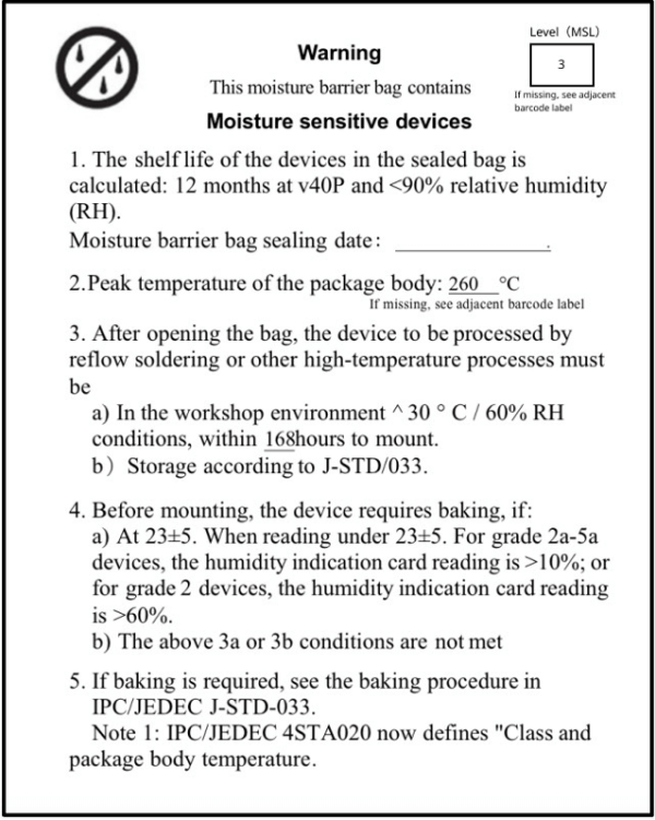
Select modules that can be SMT or in-line packaged according to the customer’s PCB design scheme. If the board is designed for SMT packaging, use SMT-packaged modules. If the board is designed for in-line assembly, use in-line assembly. Modules must be soldered within 24 hours of unpacking. If not, place them in a dry cabinet with a relative humidity of no more than 10% or repack them in a vacuum and record the exposure time (total exposure time must not exceed 168 hours).
Instruments or equipment required for SMT assembly:
- SMT Mounter
- SPI
- Reflow soldering
- Oven temperature tester
- AOI
Instruments or equipment required for baking:
- Cabinet ovens
- Antistatic high-temperature trays
- Antistatic and high-temperature gloves
Moisture-proof bags must be stored at a temperature <40°C and humidity <90% RH. Dry-packed products have a shelf life of 12 months from the date of sealing of the package—sealed packaging with a humidity indicator card.

The vacuum bag is found to be broken before unpacking.
After unpacking, the bag is found to be without a humidity indicator card.
The humidity indicator card reads 10% or more after unpacking, and the color ring turns pink.
Total exposure time after unpacking exceeds 168 hours.
More than 12 months from the date of the first sealed packaging.
Baking parameters are as follows:
Baking temperature: 60°C for reel packs, humidity less than or equal to 5% RH; 125°C for tray packs, humidity less than or equal to 5% RH (high-temperature-resistant trays, not blister packs for tow trays).
Baking time: 48 hours for reel packaging; 12 hours for pallet packaging.
Alarm temperature setting: 65°C for reel packs; 135°C for pallet packs.
After cooling to below 36°C under natural conditions, production can be carried out.
If the exposure time after baking is greater than 168 hours and not used up, bake again.
If the exposure time is more than 168 hours without baking, it is not recommended to use the reflow soldering process to solder this batch of modules. The modules are class 3 moisture-sensitive devices and may become damp when the exposure time is exceeded. This may lead to device failure or poor soldering when high-temperature soldering is carried out.
Please protect the module from electrostatic discharge (ESD) during the entire production process.
To ensure product qualification rates, it is recommended to use SPI and AOI test equipment to monitor solder paste printing and placement quality.
Please follow the reflow profile for SMT placement with a peak temperature of 245°C. The reflow temperature profile is shown below using the SAC305 alloy solder paste.

Description for graphs of curves.
A: Temperature axis
B: Time axis
C: Alloy liquid phase line temperature: 217-220°C
D: Slope of temperature rise: 1-3°C/s
E: Constant temperature time: 60-120s, constant temperature: 150-200°C
F: Time above liquid phase line: 50-70s
G: Peak temperature: 235-245°C
H: the slope of temperature reduction: 1-4°C/s
Note: above-recommended curves are based on SAC305 alloy solder paste as an example. Please set the recommended oven temperature curve for other alloy solder pastes according to the solder paste specification.
| Model | RAM | eMMC |
|---|---|---|
| DSOM-130N-1 | 2GB | 16GB |

